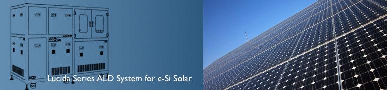
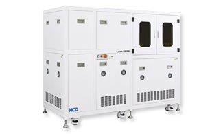
Atomic layer deposition system for surface passivation of
c-Si solar cells |
| Applications |
- Surface passivation of c-silicon solar cells
- Applications of R&D
- High throughput
: > 500 wafers/hour of 156 x 156㎟ size with 10nm thickness |
| Features |
- Al2O3 thin films with good thickness uniformity
- Advanced process kit and small volume chamber for short gas cycle times
- Extremely materialize ALD mechanism
- Small foot print
- Totally integrated process module
- Easy process control
- Minimize gas supply line length
- Cassette to cassette operation
|
| Technical specifications |
| Substrate size |
156 x 156㎟ |
| Substrate temperature |
25℃ ~ 250 ℃ |
| Precursor sources |
TMA, H2O( O3 optional) |
| Deposition uniformity |
<±2% |
| Footprint |
2375 x 950 mm |
| Compatibility |
Clean room class 10000 |
| Control system |
PLC control with PC user interface
(full auto) |
| Optional |
O3 generator |
|