Global Leader in ALD Technology

- COMPANY
- News
News
ALD IGZO application for Monolithic 3D Integration
작성자 : 최고관리자
등록일 : 22-08-09 11:20
관련링크
본문
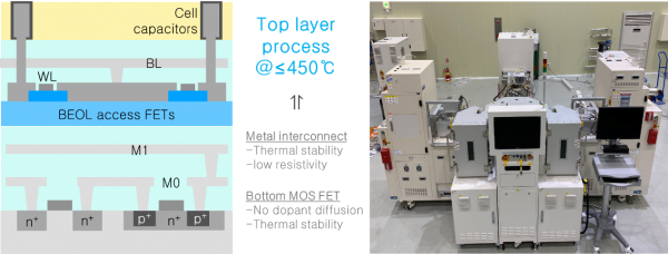
< Diagram of Monolithic 3D IC & Lucida™ S300 ALD >
Improvement of device performance and decrease of power consumption by scaling down in semiconductor industry almost have reached the physical limit. Additionally the possibility of memory’s capacitor collapsing have been increasing due to capacitor’s becoming narrower and higher so it can lead to reduce device reliability.
To escape the limit of scaling down, Monolithic 3D (M3D) technology which stacks layer by layer third dimension integration would be available instead of planar scaling. Because it is scalable, performable and economic, lots of companies, institutes and universities are actively developing for its commercialization.
There is the limitation of upper layer process temperature because dopant diffusion, property degradation and dimensional change in the lower device can happen during M3D integration. Therefore, to prevent the lower device from deteriorating, the process temperature for upper channel materials must be limited not more than 450℃. IGZO has great properties and can be processed at low temperature so applying IZGO to M3D devices has been studied and developed such as IGZO OSFET stacking on CMOS devices or RRAMs.
Recently, IGZO is being applying to capacitor-less DRAM (2T0C) because IGZO TFT has very low off current (Ioff) by long retention time.
ALD IGZO enables conformal deposition and excellent thickness controllability. Also composition control by cycle number ratio is accurate so the bilayer structure can be easily deposited. It is expected to be applied for superb M3D devices.
NCD has been developing IGZO batch IGZO-ALD system with its creative technology and it shows excellent film properties and high throughput with large area processing. LucidaTM S Series is very available for developing M3D integration of Logic, Memory and electro optics etc.
LucidaTM S Series for semiconductor is a high throughput ALD system with thermal or plasma process for 300 mm wafers and is able to deposit various oxides (HfO2, ZrO2) and metals (TiN, TaN, Ru) with excellent property and film uniformity.
